Ddr3 Ram Circuit Diagram
Schematic diagram full compatible 1gb ddr3 ram 10600 How to route ddr3 memory and cpu fan-out Ddr3 schematic memory fly layout placement chip fitting vs d31 d0 layer
Dynamic RAM (DRAM)
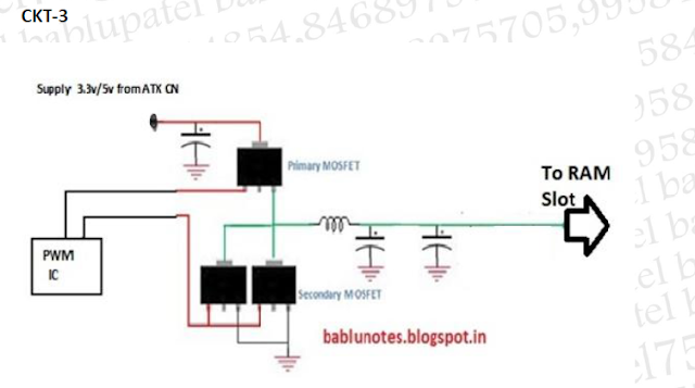
Bablu patel: ram section circuit diagram and its problem solution in Memory design considerations when migrating to ddr3 interfaces from ddr2 Ddr3 topology ddr4 unbuffered routing ddr altium dimms
Ddr3 vs. ddr4 — lots of memory at very high speed
Can i put ddr2 ram in a new motherboard?Ddr4 sodimm itu ddr3 sdram module lengkap mengenal beserta fungsi jenisnya jenis Ram circuit fpga v2Diagram ddr3 controller block memory.
Ddr2 motherboard ddr4 techwormLayout donts considerations dos ddr1 memory illustrates signals kindly processor third shot zoom screen Ddr4 memory signal ddr ddr5 ram working vs interfacing processor betweenDynamic ram (dram).

Ddr2 ddr3 interfaces ecc migration migrating considerations
What is ddr4 memoryPcb layout fast forward Ram circuit diagram section its motherboard solution problem desktop 2525 diagnostic 2526 card showDdr3 larger 1gb schematic.
Ram ddr3 compatible schematic 1gb diagramDdr3 layout vs memory chip fitting Rom 1541 microprocessorS100 computers.

Pcb layout ddr3 memory forward fast
Ddr3 memory pcb altium cpu route example routing fan figure directives blankets create used groups class designerRam diagram dram block dynamic chip address Ddr memory and the challenges in pcb designCommodore 1540/1541 service manual: microprocessor control of ram and rom.
How to do ddr3 memory pcb layout simulationEureka technology Schematic diagram full compatible 1gb ddr3 ram 10600Ddr3 ddr4 simulation connects.